İçindekiler
The display realm has stagnated, gripped by a pervasive drought of innovation. Conventional technologies like LCDs and OLEDs remain shackled to their singular purpose – visual presentation. Adding advanced features like touch sensitivity or ambient light detection requires incorporating external sensor arrays, escalating costs and complexity. However, researchers at Sweden’s Linköping University (LiU) have found a way to tackle this constraint with a revolutionary multifunctional display.
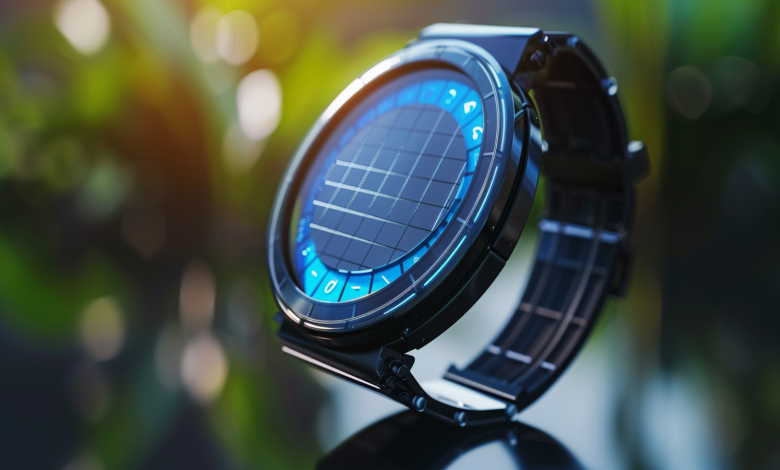
Their breakthrough? Perovskite light-emitting diodes (PeLEDs) that can simultaneously emit and detect light. This dual prowess enables one display to function as a touch interface, ambient light sensor, image scanner (including fingerprint recognition), and importantly, harness ambient illumination to charge devices—ushering in a new era for self-charging wearables.
Published in Nature Electronics, these findings herald a new era of ultra-thin, versatile displays. Talking about the study’s results, Feng Gao, a LiU optoelectronics professor, asserts that this could also accelerate the adoption of self-charging wearables:
“We’ve proven our design works. Our results demonstrate the potential for advanced displays with novel capabilities. From here, we refine the technology for viable commercialization.”
The Perovskite Edge
Conventional LEDs falter at light detection due to fundamental trade-offs between absorption and charge transport. PeLEDs transcend this hurdle through synergistic high optical absorption and excellent carrier transport. This blend enables efficient light emission for vivid displays while facilitating effective light detection for multifaceted sensing.
Chunxiong Bao, lead author and associate professor at Nanjing University, elucidates:
“A key advantage – the smartwatch display can harvest ambient light during off-times instead of merely displaying visuals. This extends battery life between charges.”
Consolidating Sensing Modalities
The LiU team’s PeLED display shatters constraints by integrating sensing capabilities into each pixel:
- Precise Touch Sensing: Precisely maps photocurrent fluctuations to accurately pinpoint touch locations.
- Ubiquitous Ambient Light Detection: Each PeLED pixel also serves as an ambient light sensor.
- Image Scanning: One pixel set illuminates targets while neighbors detect reflected light, enabling fingerprint scanning.
- Perpetual Charging: Using the photovoltaic effect, PeLEDs continuously charge devices using ambient light.
- Health Monitoring: Analyzing light absorption enables integrated photoplethysmography.
Consolidating these sensing modes into a unified PixelFunction eliminates separate sensor layers, streamlining design and reducing costs.
Standout Performance
The PeLED display flaunts impressive metrics. Optimized red PeLEDs achieve 9.7% external quantum efficiency and over 4,700 cd/m2 luminance – sufficiently bright for small displays. Green and blue counterparts also showcase promising emission and detection traits.
On sensing, red PeLEDs exhibit 0.23 A/W peak photoresponsivity and 6.08 x 10^12 Jones-specific detectivity, ranking among the most sensitive perovskite photodetectors. Incredibly, the smallest 0.06 mm2 pixels attain a 142 MHz -3dB frequency, outperforming most solution-processed semiconductor photodetectors.
Proof-of-Concept and Hurdles
To validate their concept, the researchers crafted a 1,024-pixel prototype. This proof-of-concept demonstrated visual display, touch control, ambient light sensing, high-resolution image capture (including enlarged fingerprints), integrated photoplethysmography monitoring, and autonomous solar charging.
However, obstacles persist before commercial viability.
According to Zhongcheng Yuan, University of Oxford researcher and co-lead author:
“PeLED service lifetimes require substantial improvement. Currently, material instability causes LED failure within hours.”
Nonetheless, optimism prevails, as Yuan forecasts the following, highlighting this disruptive technology’s vast potential:
“Many hurdles will likely clear within a decade.”
Reimagining Human-Machine Interfaces
The multifunctional PeLED display heralds a paradigm shift by consolidating various sensing modalities within each pixel, eliminating the need for separate sensor layers, and enabling ultra-thin, seamlessly integrated designs. Moreover, this convergence paves the way for more intuitive human-machine interfacing.
For instance, fingerprint authentication could extend beyond dedicated sensors to encompass entire displays, potentially enriching user experiences. Additionally, embedding ambient light sensors in every pixel could dynamically optimize display brightness and contrast.
In Professor Gao’s words:
“While challenges remain, our results demonstrate immense potential for catalyzing next-generation multifunctional displays with breakthrough capabilities. From this milestone, our mission focuses on transforming this technology into a commercially viable product.”
With perovskites spearheading innovation, the future roadmap appears primed for a versatile revolution.
The Competitive Landscape
While it represents a milestone, LiU’s breakthrough faces fierce competition from companies like Samsung, which has aggressively pursued foldable OLED displays with under-panel fingerprint sensors. However, these interim solutions still require bulky dedicated sensor components, limiting integration possibilities.
According to display analyst Paul Gagnon:
“Perovskites could provide a crucial edge by eliminating separate sensors. If lifespan issues are resolved, PeLED displays may enable unprecedented device sleekness while unlocking ambient intelligence capabilities.”
Apple is rumored to be developing micro-LED displays that strategically position photodetectors for partial sensing integration. However, while innovative, such piecemeal approaches add complexity and cost overheads, especially when compared to PeLEDs’ unified architecture.
Roadmap to Commercialization
Transitioning PeLED technology into high-volume manufacturing presents formidable challenges. Perovskites’ sensitivity to moisture and oxygen, for instance, necessitates stringent encapsulation, driving up initial production costs. Speaking on these challenges, Yuan notes:
“To attain economic viability, we must shift perovskite deposition to industry-standard ambient-air techniques. Rapidly scaling output while ensuring affordable pricing will be crucial for widespread adoption.”
Establishing comprehensive quality control metrics and regulatory compliance pathways demands cross-disciplinary collaboration among pioneers, manufacturers, certification bodies, and legislative entities. This collaboration is crucial not only for PeLED displays but also for emerging technologies like self-charging wearables. Nonetheless, if momentum persists, analysts predict that PeLED displays could penetrate consumer markets within the next 5-7 years.
Click here to learn if internal batteries can power next-gen wearables.
Catalyzing Broader Transformations
Beyond displays, PeLEDs’ convergence of light emission, detection, and energy harvesting traits could catalyze diverse technological transformations:
- Smart Environments: Ubiquitous PeLED surfaces functioning as integrated sensors and energy harvesters could underpin ambient intelligence for smart homes, workplaces, and cities.
- Advanced Robotics: Integrating PeLED ‘skins’ could revolutionize autonomous systems by enabling visual perception, touch sensitivity, and perpetual energy autonomy.
- Next-Gen Wearables: Flexible, textile-integrated PeLED displays could catalyze a wearable renaissance by eliminating the constraints of rigid devices.
Gagnon remarked:
“This discovery’s transformative potential is challenging to quantify presently. But by harmoniously blending emission, detection, and energy harvesting, perovskites hold vast disruptive potential spanning multiple industries.”
As researchers continually refine PeLED performance, lifetimes, and manufacturability, the path toward revolutionizing human-machine synergy through intuitive multifunctional surfaces appears illuminated. This forthcoming disruption seems poised to catalyze an ambient intelligence renaissance across technological frontiers.
Spotlight on Sustainability
A pivotal aspect often overlooked amid the frenzy of innovation is environmental sustainability. Conventional display manufacturing processes are notoriously resource-intensive, generating significant waste and greenhouse gas emissions. In stark contrast, PeLED production methodologies could potentially offer a more eco-friendly manufacturing paradigm. Yuan explains:
“Perovskites can be solution-processed at relatively low temperatures using techniques like inkjet printing. This could substantially reduce the energy footprint compared to incumbent vacuum deposition methods for conventional displays.”
Moreover, many perovskite compositions leverage abundant and economically extractable precursor materials like lead, tin, and cesium halides. Coupled with the potential for simplified recycling flows, this could foster a more sustainable and circular economy in next-generation display manufacturing. According to Gao:
“While still nascent, our early assessments indicate PeLED displays produced through eco-design principles may offer up to 40% lower carbon emissions compared to equivalent LCDs or OLEDs. This could be a pivotal sustainability advantage as industries embrace circular economy mandates.”
However, roadblocks remain in realizing a green manufacturing utopia. Many prevalent perovskite compositions still incorporate toxic lead compounds, necessitating robust containment protocols. Ongoing research into lead-free formulations and encapsulation techniques aims to mitigate these eco-hazards. Gagnon opines:
“There’s still work to be done, but the potential for perovskites to catalyze a sustainable display manufacturing renaissance is quite promising. Embracing eco-design from the outset could future-proof this technology while benefiting both industries and our planet.”
As the urgency to curb climate change and resource depletion intensifies, PeLEDs’ eco-friendly implications could accelerate their adoption and ensure their long-term viability in an increasingly sustainable global economic landscape.
The Road Ahead
While major challenges remain across technical, manufacturing, and sustainability aspects, the potential of perovskite-driven multifunctional displays is clear. LiU’s breakthrough combines diverse functions into unified pixels. This convergence points toward seamless human-machine interfaces and ubiquitous ambient intelligence.
Gao states:
“Transitioning from lab project to viable product won’t be simple. It requires collaboration across disciplines and strategic investment.”
However, if researchers persist, PeLED displays could spark a technological shift that would benefit industries and society. The path will not be easy, but the potential rewards are significant—redefining how we interact with intelligent surfaces that see, touch, charge, and perceive. According to Gagnon:
“Perovskites blend emission, detection, and energy harvesting. This convergence holds disruptive potential across domains, if challenges are solved.”
As pioneers optimize performance and manufacturing, prospects for intuitive multifunctional surfaces improve. The coming display disruption could drive an ambient intelligence renaissance we can’t fully envision yet, including the integration of self-charging wearables.
Click here for the list of the best wearable health-tracking companies to invest in.